When designing PCBs for wave impedance, the following must be known:
1. Materials with different thicknesses have different dielectric constants. The constants for materials we use can be seen here, here and here.
2. About the operating frequency of the interface. The relevant dielectric constant can be found from the previously linked data sheet.
3. The nominal copper thickness of the inner layers decreases by 3 µm in our processes. E.g., the copper thickness in the case of an 18 µm foil inner layer will be 15 µm after production. Meaning that when calculating wave impedance, 15 µm must be entered into the program.
This value depends on the processes used by the producer and may differ from our 3 µm.
4. The copper thickness of outer layers increases, due to galvanic copper plating, by at least 35 µm. Meaning that both base foil and galvanic copper plating must be taken into consideration (12 µm + 35 µm =47 µm).
5. Depending on the topography or uniformity of the copper area of the outer layers, the copper thickness on tracks or sparser copper areas can be up to twice as high when compared to a filled area.
6. During the etching process, the width of the tracks decreases, at minimum, by the thickness of the base foil.
7. Regarding the availability of necessary inner layers and prepegs. One should determine during the design stage, which materials are available at the warehouse and take this into consideration. Our selection of materials can be viewed here. In case your required build up and the build up offered by the supplier do not match, please recalculate the wave impedance using the newer build up!
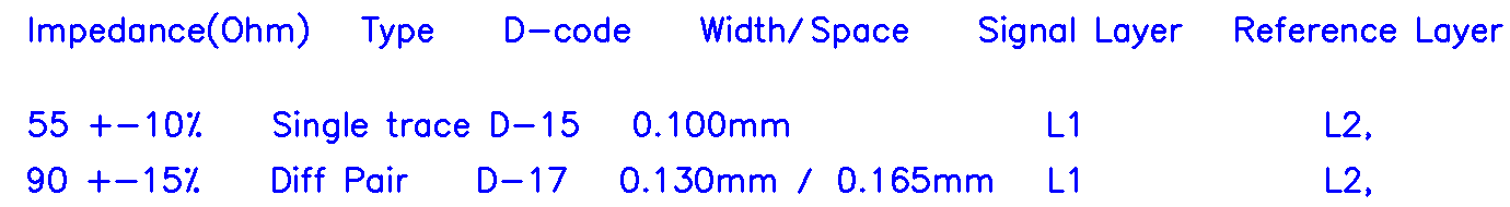
8. Always add to the files a specification that would show the type of wave impedance (single, diff pair); impedance value in ohms and tolerance; values for signal and support layer (signal, ref); and track width and gap (D-code would also be helpful). One possible specification has been given below: