Here we have collected the most frequently asked questions and topics that are being asked literally every day, over and over.
1) Mask openings need to be reduced? Why? How much?
This is something we can fix for you if you give us written permission to do so.
Too large mask openings can constitute a problem in the later soldering process – without properly reduced mask openings there is danger of a “solder bridge” between metallized areas / pads / wires etc.
This may result in an unwanted connection and shorts. There is no specific numerical value we can give to the question “How much exactly do you decrease mask openings”? It is all done on a case by case basis, sometimes it can controversially mean that we need to enlarge opening in specific locations. We do it as little as possible and as much as necessary, all related to our own in-house know-how and 20 years of experience.
Mask openings need to be corrected:
Correct mask openings:
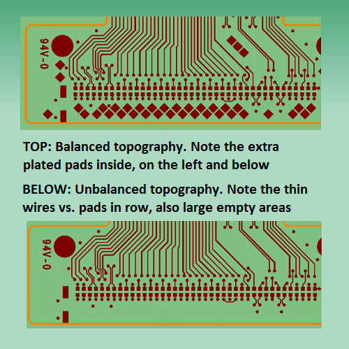
2) Unbalanced topography? What does it mean and what is the worst case scenario? How do I “balance” it?
Equalizing topography means balancing the copper layer. Significant differences in the copper area distribution, a large copper plane on one side and narrow tracks on the opposite side, will cause a unbalanced plating result during the galvanizing process. Copper thickness can be up to twice as thick on the tracks compared to the plane. In the worst case scenario this will lead to merged metallized areas/pads/wires etc. Different plating thickness across the board in itself is already an obvious problem regarding impedance control.
Possible solutions:
1) Add metallized planes where possible (opposite direction of existing ones)
2) If boards are panelized, give us permission to metallize the frames
See the illustrations below for visual description of the issue:
All green areas are copper. Note the total difference in the coverage of the left and right
sides of the board.
3) Milling cuts the copper? What can happen?
Depending on how seriously and where the cutting path interferes with the metallized areas, this issue can be either cosmetic or a major problem. Usually the open cut copper edges are slightly lifted up by the router as it cuts through the material (also known as “burrs” – very slight protrusions around the router path) – This can create problems if the board has to go into an automatic soldering machine, where it can interfere with the proper and tight stencil application on the board. We will always inform you of this type of problem and recommend for you to fix it. Regardless, you need to take full responsibility for your design when giving us a “don’t stop, produce” written order.
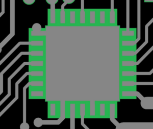
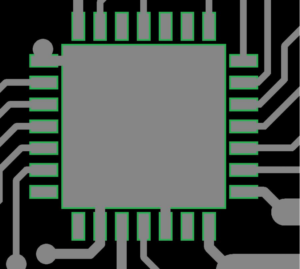
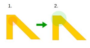
4) “There is danger of a mask pocket”? What does it mean and why is it dangerous?
Mask pocket = mask over via on one side only, with the other side of it being open, creating a closed “pocket”. Why this is sloppy design: making PCBs involves enormous amounts of chemical solutions the board has to go through. These solutions are almost impossible to wash out of mask pockets with 100% certainty. The chemical leftovers inside the pocket will create a plethora of unexpected problems later on in the production process – in other words, contamination. This will most likely influence the finishing of the affected areas. Please design smart – do not leave mask pockets anywhere. See IPC standard image below:

5) “There is a resist pocket on your board”? What does it mean and why is it dangerous?
The general method of manufacturing printed circuit boards involves a method where copper foil is coated with photo-resist, intended to be partially removed later.
In the developing-process, the light-sensitive resist is exposed to light in order to create a design pattern. The resist outside of the pattern then is removed and the unwanted copper etched out.
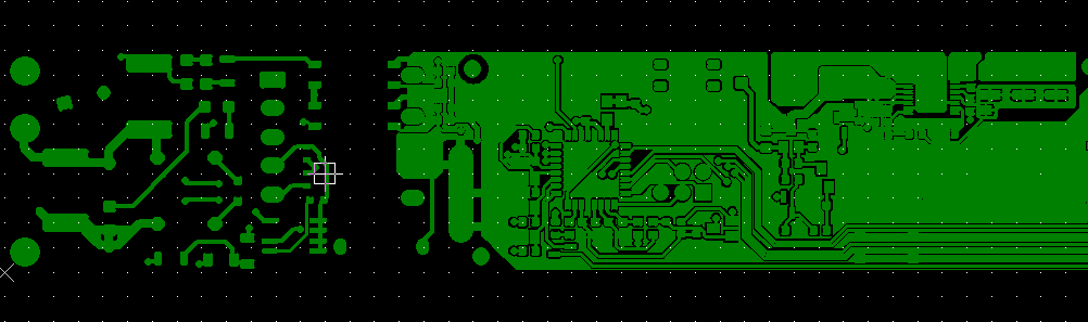
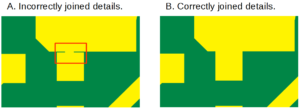
If there are sharp angles or too narrow gaps left in the design, there is a risk that unneeded resist-material gets stuck and consequently comes loose in later production stages. This can result in unwanted shorts. To avoid that, we ask our customers to correct their design, avoiding sharp angles and taking care that no design elements are poorly joined.
Sample of poorly joined details, figure A. There is no need to leave strips like the ones shown in the red frame. Same place corrected is shown on figure B.
6) Why do the single boards or panels have to have rounded corners?
To maintain maximum safe transportation and storing all boards are packed airtight in the anti-static bubble wrap. The corners are rounded to avoid sharp points pricking the bubble wrap of the parcel during handling.
Should you need the boards with sharp corners, please order them in panel (V-scored and framed) or add a frame at least 5mm wide intended to be separated with V-cut to opposite sides of the board.
7) Drill depth limits, Aspect Ratio – what does it mean?
Aspect ratio is the ratio between the drilling depth and the drill diameter. At Brander Electronics the aspect ratio for through holes is 1:16, meaning that it is not possible to drill through holes with a depth higher than 16x the drill diameter. As an exception to the rule, 0.1mm drills have an aspect ratio of 1:12, being able to drill only as deep as 1.2mm.
For blind vias it is vital to maintain an aspect ratio of 1:1. It means that if blind drills are needed, the drilling depth has to be less than or equal to the drill diameter. Please remember this detail when planning a stackup for a board with blind vias.