Here one can compile constructions that use buried and/or blind vias. Brandner Electronics makes blind vias through mechanical drilling. The following example uses a 4-layered PCB. First, choose the final number of board layers:
![]()
Then determine the structure of blind and/or buried vias.
In order to add blind vias from the top layer (TOP;layer 1) to the first internal layer (layer 2), choose the following structure:
![]()
In order to drill blind vias from the bottom layer (BOT; layer 4) to the bottom internal layer (layer 3), choose the following:
![]()
In order to make blind vias from both top and bottom layers (TOP; layer 1; BOT; layer 4), use the following structure:
![]()
In the case of buried vias, please note that buried vias can currently only exist between the outermost internal layers, which, in the case of a 4-layered PCB, means layers 2 and 3; in the case of a 6-layered PCB, layers 2 and 5, etc.
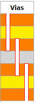
To make a build up with blind and buried vias, choose the following construction solution:
![]()
Next, choose the minimum drill diameter for both buried and blind vias. Please note that the blind via aspect ratio – i.e. drilling depth divided by drill diameter – cannot exceed 1:1! If the aspect ratio is exceeded, the program displays an error message.
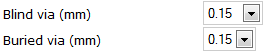
You can see the results on the graphic depiction of the package on the right:
Next, you can replace internal and prepregs or choose the construction suitable for your design. Don’t forget to save the package and send it to Brandner Electronics along with your order.