Every day we ship a number of packages containing high-quality printed circuit boards (PCBs) from our building. On February 12 and 19, we also sent out invaluable know-how from our building, by sharing it with our clients.
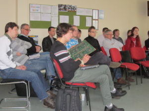
On those days, we hosted a seminar with the purpose of bringing the client closer to the principles behind, and the actual construction of, PCBs.
The discussions that arose, the frank conversation with our chief technologist, and a tour of the factory, raised the level of awareness regarding the actual production process of PCBs to a whole new level for many of the participants.
Representatives from Tallinn University of Technology were surprised to see the actual route that a project they have sent takes before it is packaged in the physical form of a PCB and shipped off.
Young go-getters from Formula Student got to see the actual PCB production process and the principles supporting them in their studies as well as the construction of this year’s new formula model. This know-how and experience will also provide a foundation for them to start their own electronics-related businesses, either during their studies or after graduation.
For the so-called ‘old hands’ this was the place for discussing the events of the day and sharing their experiences. The EstCube folks, who have already visited us before and have dealt with electronics construction and R&D for years, found the seminar to be a confirmation of the fact that Brander continues to operate at a high level and is ready to help them with PCBs in their new projects.
Brandner thanks all participants.
You are invaluable to us.